Parallel to UART Adapter
Project completed: January 2022
Summary
In this project, I designed and implemented a parallel to UART adapter, in Verilog.
Background
I was experimenting with FPGA’s. During this process I wanted to send serial data. There was no intellectual property available in either Lattice Diamond or Xilinx Vivado for this task. As a result, I decided to create my own.
Circuit Design
In this section, I am going to explain the circuit used to generate the serial output. I used a program called Logisim Evolution to verify the correct operation of the circuit. The Logisim Evolution file can be found in my GitHub repository (link).
Complete Circuit
The complete parallel to UART circuit is shown below.
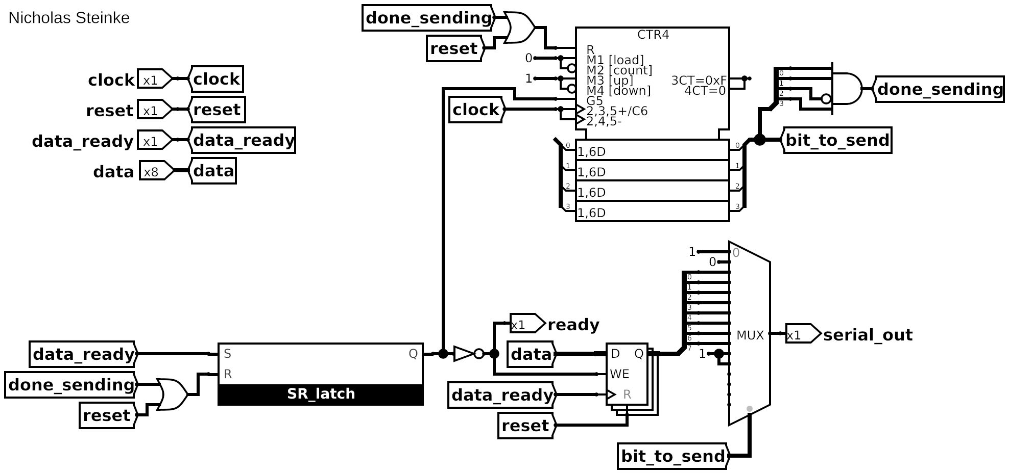
Data Latch
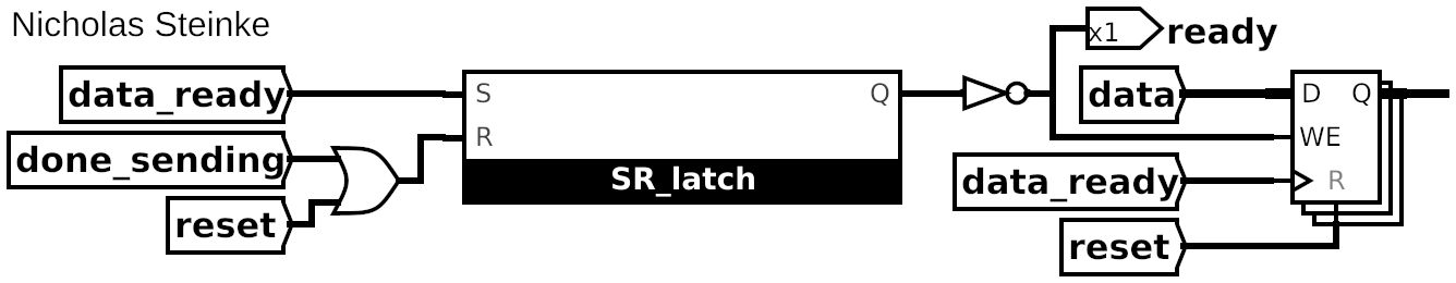
The first part of the circuit is the input data latch. The point of this circuit is to latch the input data when the data_ready line goes high and prevent any new data from being latched when the rest of the circuit is sending serial data.
The circuit use two main components to achieve the goal. They are an 8-bit data latch and a SR latch. During a reset, the SR latch is cleared. This enables the data latch. When data_ready goes high, the data is latched and the SR latch is set. This causes the latch to be disabled. As a result, no new data can be latched. The only way to clear the SR latch is when a future part of the circuit indicates it is done sending the data.
Bit to Send Selection
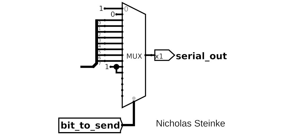
This part of the circuit is responsible for selecting the correct bit to send.
Serial data has the following sequence.

The bit to send selection circuit is built around a 4-bit MUX. The MUX inputs 0 and 11 handles the idle condition. The reason why input 11 on the MUX is also a value of 1 comes from the propagation delay needed to reset the counter. During this time, the MUX will be using input 11. This makes sure the value is valid. The MUX inputs 1 and 10 handles the start and stop bit respectively. The MUX inputs 2 through 9 are the data bits.
Bit Counter
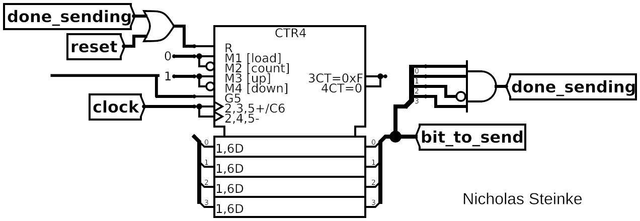
The final part of the circuit is the bit counter. This circuit handles choosing which bit to send.
The circuit is a simple, 4-bit, binary counter. The input clock is at the desired serial output frequency. The enable input comes from the SR latch used as part of the data latch circuit. Finally, there is a comparator on the output to reset the counter.
Verilog Code
The Verilog code which implements the parallel to UART adapter can be found on my GitHub repository (link). I tested the code using Icarus Verilog and implemented the circuit on an FPGA using Xilinx Vivado. Both implementations worked perfectly.
The code and Logisim Evolution files can be found here